TFFThin Films Finland
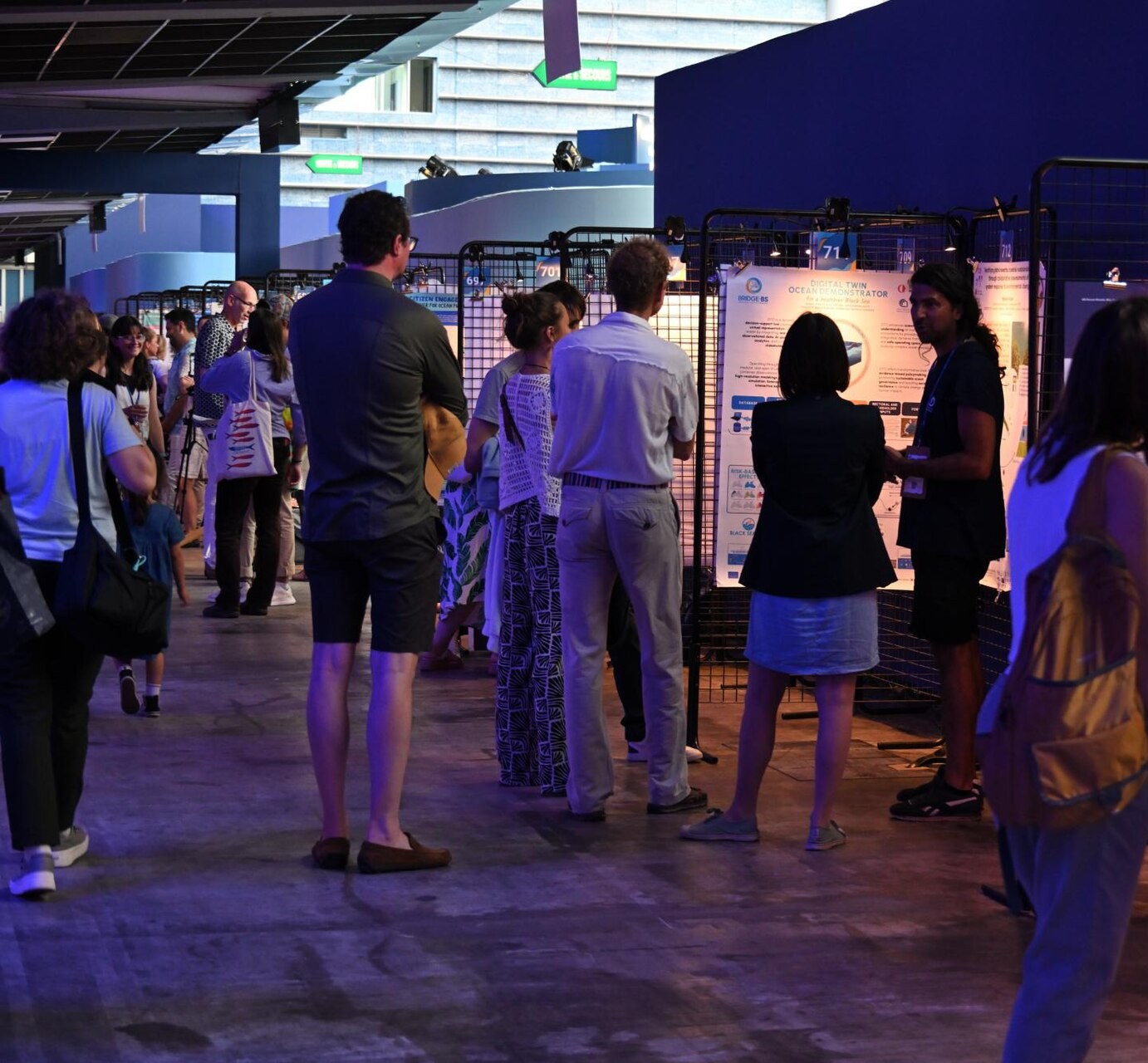
Delegates walking among the posters at a scientific poster session
One Ocean Science 2025 · S. Lesbats / Ifremer · CC BY 4.0
Autumn 2027 · Finland

THIN
FILMS
FINLAND

A Finnish effort with a Nordic soul — welcoming everyone

Gathering Finland's and the Nordic region's thin film community.

A two-day scientific conference on thin film deposition and characterisation, in autumn 2027.

Thin Films Finland · Autumn 202701 / 16
TFFThin Films Finland
01 · The gap
The current landscape

Nordic thin film science is world-class — and scattered.

Researchers split their year between technique-specific meetings abroad. There is no single Nordic conference that brings all thin film methods together — and none in Finland.

Fragmented
One meeting per technique, rarely in the Nordics
Costly
Students and small groups can attend only a few
Siloed
ALD, PVD, CVD and thin film characterisation people from the Nordic countries have limited events to meet
Thin Films Finland · Autumn 202702 / 16
TFFThin Films Finland
02 · Why Finland
Why here

A substantial Nordic thin film community.

Not too small, not too large — a community at a scale that is manageable and suitable for TFF to happen.

Thin film research output
A steadily growing body of work, year after year
FinlandNordic countries

Every year, dozens of thin film related papers are published from Finland.

Even more in Nordic countries combined.

The number of speakers and attendees — the audience for this event is the ideal size, not too big.

The Nordic thin film community continues to grow, year after year.

Thin Films Finland · Autumn 202703 / 16
TFFThin Films Finland
02 · Why Finland
A national research community

Thin film expertise spans Finland.

Research community
University of Helsinki
Helsinki
Aalto University
Espoo
VTT
Espoo & national
Tampere University
Tampere
University of Jyväskylä
Jyväskylä
University of Turku & Åbo Akademi
Turku
LUT University
Lappeenranta
University of Oulu
Oulu
University of Eastern Finland
Joensuu & Kuopio
Industry
Beneq
Espoo
Applied Materials (ex-Picosun)
Espoo
ASM Microchemistry
Espoo
Optorun
Finland
Chipmetrics
Joensuu
Canatu
Espoo
Okmetic
Vantaa
Murata
Salo

This Finnish network is only part of the picture: across Sweden, Denmark, Norway and Iceland, many more research groups broaden the Nordic thin film community.

Thin Films Finland · Autumn 202704 / 16
TFFThin Films Finland
03 · The event
The event

A two-day, non-profit scientific conference.

The first edition takes place in autumn 2027 in Finland, with sessions covering the major thin film deposition techniques and thin film characterisation methods.

2 daysKeynote each morning, three session blocks a day
3–4 roomsParallel session rooms + plenary keynotes
24 sessions≈ 96 talks across 14 technique families
PostersPoster session scattered through the area to invite conversation
Thin Films Finland · Autumn 202705 / 16
TFFThin Films Finland
04 · Scientific scope
Scientific scope

Every technique, one conference.

ALD & PEALD
Thermal and plasma-enhanced ALD
Area-selective
Area-selective deposition
ALE
Atomic layer etching
CVD
Thermal chemical vapour deposition
PECVD
Plasma-enhanced CVD
MOCVD
Metal-organic CVD / MOVPE
MBE
Molecular beam epitaxy
PLD
Pulsed laser deposition
PVD
Sputtering, HiPIMS, arc
Evaporation
E-beam and thermal evaporation
Wet processes
Spin coating, sol-gel, spray, electrodeposition
2D & emerging
Graphene, TMDs, perovskites
Characterisation
Ellipsometry, XRR, XPS, AFM, in-situ
Modelling
Simulation and process modelling
Industry
Applications & new technologies
Thin Films Finland · Autumn 202706 / 16
TFFThin Films Finland
05 · Draft programme
Programme outline · 2 days · 3–4 rooms
Day 1
Room ARoom BRoom CRoom D09:00
Opening keynote · plenary
09:45
Coffee
10:15
ALD I · Thermal ALD
CVD I
PVD I · Sputtering
Characterisation I
11:45
Lunch
13:00
ALD II · PEALD
CVD II
PVD II · Sputtering & HiPIMS
Industry talks I
14:30
Coffee
15:00
Area-selective deposition
PECVD
E-beam & thermal evaporation
Wet processes I
16:30
Posters
Day 2
Room ARoom BRoom CRoom D09:00
Keynote · plenary
09:45
Coffee
10:15
ALE · Atomic layer etching
MOCVD / MOVPE I
MBE
Characterisation II
11:45
Lunch
13:00
2D & emerging materials
MOCVD / MOVPE II
PLD
Industry talks II
14:30
Coffee
15:00
Modelling & simulation
Characterisation III
Industry talks III
Wet processes II
16:30
Student awards & closing

24 sessions of 90 min · each ≈ 1 invited talk (30 min) + 3 contributed talks (20 min) · ≈ 96 talks + 2 keynotes + posters

Thin Films Finland · Autumn 202707 / 16
TFFThin Films Finland
06 · Students
Investing in the next generation

Attendance is free of charge.

Attendance is free of charge for everyone, alongside a full poster session and awards for the best student oral and poster contributions — funded by exhibitors and sponsors.
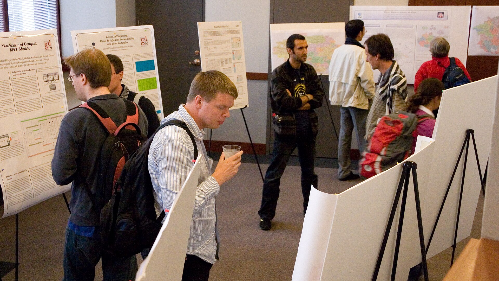
Researchers discussing work during a scientific poster session
David Eppstein · CC BY-SA 3.0
01Best student oral presentation
02Best student poster
03Best poster per technique family
Thin Films Finland · Autumn 202708 / 16
TFFThin Films Finland
07 · Format
One floor, one community

Sessions, posters and coffee in one place.

Three to four session rooms and a plenary, with the poster session and tabletops scattered through the same area so participants keep meeting between sessions.

PLENARY ~300 · ROOMS ~80–120
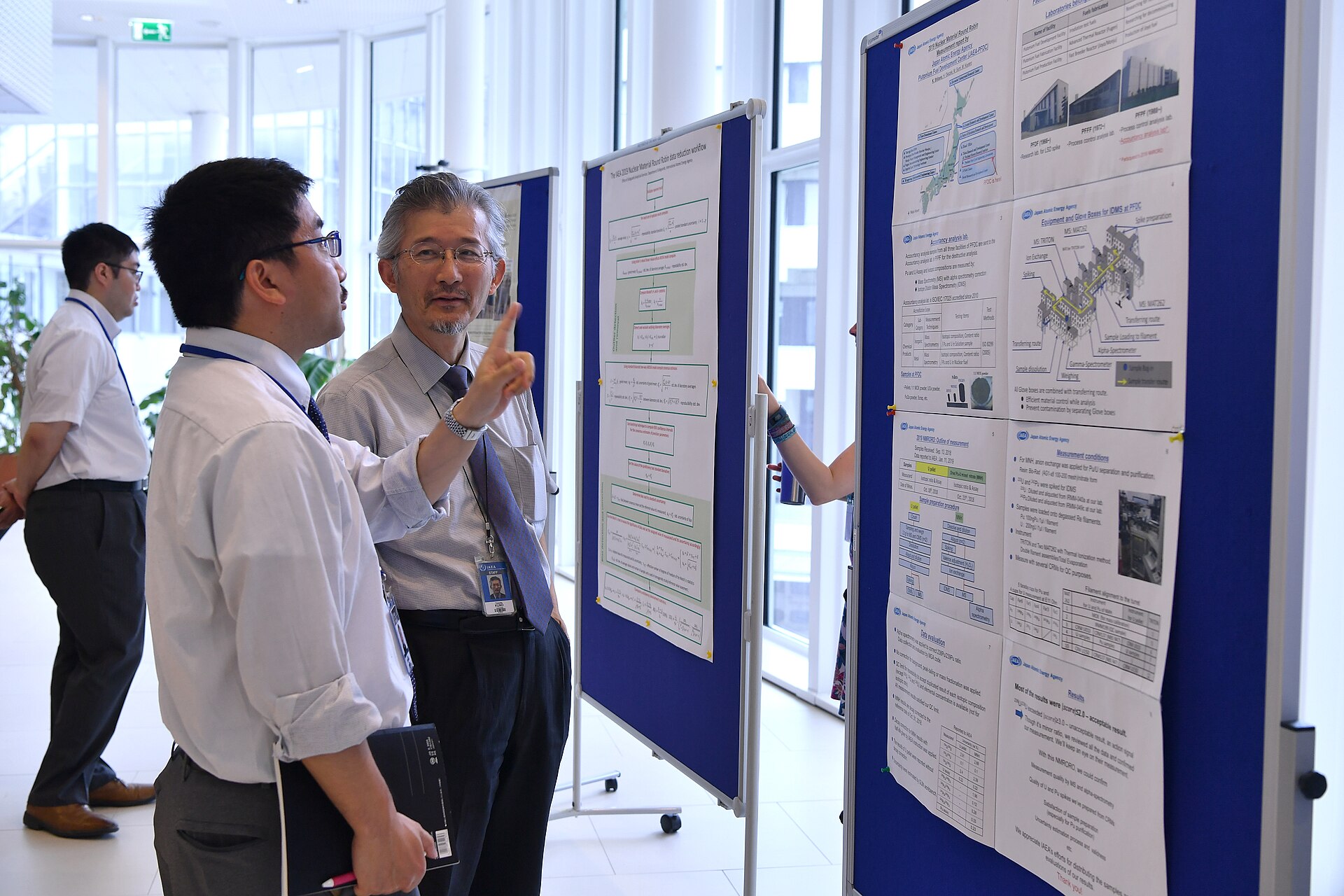
Delegates viewing research posters in a bright conference hall
IAEA Imagebank · CC BY 2.0
Floor concept
Room A
Room B
Plenary
Posters · Tabletops · Coffee break
scattered to encourage conversation
Room C
Room D
Thin Films Finland · Autumn 202709 / 16
TFFThin Films Finland
08 · Take part
Open to everyone

Researchers, students and industry in one place.

How you can take part
  • — Researchers: submit a talk or a poster
  • — Students: compete for the student awards
  • — Companies: book a tabletop or become a sponsor
  • — Everyone: attend free of charge
Thin Films Finland (TFF)
  • — Independent organiser, owns the event brand
  • — Runs logistics, website, submissions, registration
  • — Secures a few tabletop exhibitors and sponsors, and handles their finances
  • — All income, after expenses, is donated to the hosting university

TFF is an independent, non-profit event built for the Nordic and Baltic thin film community.

Thin Films Finland · Autumn 202710 / 16
TFFThin Films Finland
09 · Finances
A self-funding event

Free for every attendee.

Attendance is free of charge for everyone. A few tabletop exhibitors and sponsors — equipment and consumables makers — fund the event and widen its audience.

Attendance
StudentsFree
Academic delegatesFree

TFF is a non-profit event. All income, after all event expenses, is donated to the hosting university — which decides how it is used.

Thin Films Finland · Autumn 202711 / 16
TFFThin Films Finland
10 · Timeline
The road to autumn 2027

From now to opening day.

Q4 2026
Dates and venue
Q1 2027
Scientific committee; website and call for abstracts
Q2 2027
Keynotes; registration and industry support
Summer 2027
Review submissions and confirm programme
Autumn 2027
Thin Films Finland — first edition
Thin Films Finland · Autumn 202712 / 16
TFFThin Films Finland
11 · Get in touch
Stay in touch

See you
in autumn 2027.

Step 01
Follow the call for abstracts
Step 02
Plan a talk or a poster
Step 03
Get in touch about tabletops and sponsorship

Israel Ayala · israel@ayala.fi · +358 50 405 5668

Thin Films Finland · Autumn 202713 / 16
TFFThin Films Finland
Mock-up · what-if

Day 1 · what-if programme Mock-up

37 talks

Mock-up: what TFF could have looked like with real 2025–2026 papers by Nordic and Baltic authors. No one listed has been invited or has agreed to speak.

09:00 KEYNOTE · W. M. M. (Erwin) Kessels (NL) — Atomic Layer Deposition
ALD I · Thermal ALD10:15
10:15 Princess Stephanie Llanos FI · invited
Impact of powder and electrode ALD coatings on the performance of intercalation cathodes for lithium–ion batteries
10:45 Georgi Popov FI
Recent trends in thermal atomic layer deposition chemistry
11:05 Sara Pakseresht FI
Atomic layer deposition for protecting lithium metal anodes to high-voltage battery applications
CVD I10:15
10:15 Anastasios Karakassides FI · invited
The impact of ferrocenium as a catalyst on the chiral distribution of single-walled carbon nanotubes in floating-catalyst chemical vapor deposition synthesis
10:45 Zhenyu Xu FI
Controllable growth transition from single-walled to double-walled carbon nanotubes using sulfur in an aerosol CVD reactor
11:05 Abu Taher Khan FI
High-performance field-effect transistors with semiconducting-rich single-walled carbon nanotube bundle
PVD I · Sputtering10:15
10:15 Yan Lin FI · invited
Establishing Ohmic contact with ultra-thin semiconductor layer through magnetron sputtering for dendrite-free Zn metal batteries
10:45 Jarkko Etula FI
Hierarchical magnetic self-assembly of few-nanometer rutile TiO 2 particles via magnetron sputtering
11:05 Milad Ghaemi FI
Crystallization dynamics and interfacial structure during growth of thin Nb films on Cu by high-power impulse magnetron sputtering: A molecular dynamics study
Characterisation I10:15
10:15 Aleksi Kamppinen FI · invited
Spectroscopic Ellipsometry Characterization and Radiative Limit Modeling of Bismuth‐Based Perovskite‐Inspired Absorbers for Indoor Photovoltaics
10:45 Masoud Rastgou FI
Comparison of thin-film thickness measurements using ellipsometry and reflectometry with uniform samples
11:05 M. Fiaz Khan FI
Effect of Fe ion beam irradiation on structural, surface, optical, and electrical properties of ZnO thin films prepared by radio frequency sputtering
11:25 Anish Philip FI
Conformality of atomic/molecular layer deposited lithium terephthalate thin films
ALD II · PEALD13:00
13:00 Amit Tewari FI · invited
Direct PEALD Deposition of a HfO2 Gate Dielectric without the Passivation for TFTs on Rigid and Flexible Substrates
13:30 Priyanka Goel FI
Thermoelectric and electronic transport properties of thermal and plasma-enhanced ALD grown titanium nitride thin films
13:50 Amit Tewari FI
Influence of In Situ Atomic Layer Annealing and Plasma-Enhanced Atomic Layer Deposition Techniques for Low-Temperature Deposition of HfO2 High-κ Gate Dielectrics
14:10 Jaakko Julin FI
Oxidant-Free Atomic Layer Deposition of SnO2 Using Complementary Metal Precursors
CVD II13:00
13:00 Sergei Malykhin FI · invited
Effect of electron-beam irradiation on the luminescent properties of nitrogen-related defects in the needle shaped diamond
13:30 Alexander V. Generalov SE
One-step synthesis of graphene containing topological defects
13:50 Katharina Hauer NO
Study of effects of fractal apertures on diamond growth
PVD II · Sputtering & HiPIMS13:00
13:00 Joel Fischer SE · invited
An ionisation region model of reactive high-power impulse magnetron sputtering of Ti in an Ar/N 2 atmosphere
13:30 Rui Shu SE
nc-MeB2/a-MPEA structured (HfMoNbZr)xTi1-xBy films for enhanced hardness, toughness and tribological performance
13:50 Smita Gangaprasad Rao SE
Corrosion resistance of coated aluminum bipolar plates for proton exchange membrane fuel cells
Industry talks I13:00
13:00 Remuel Isaac M. Vitto FI · invited
Interfacial engineering of conformal titanium oxide nanofilms on porous carbon supercapacitor electrodes via atomic layer deposition
13:30 Basit Ali FI
CeOx enhanced electrochemical performance of LiNi0.80Mn0.1Co0.1O2 cathode active material for Li-ion batteries
13:50 Safdar Muhammad FI
MgF2-based conformal antireflection coatings on highly curved lenses by atomic layer deposition
14:10 Sundas Ismaeel FI
Area selective atomic layer deposition of ruthenium with pinacolborane as a small molecule inhibitor
Area-selective deposition15:00
15:00 Heta-Elisa Nieminen FI · invited
In Vacuo Studies on the Mechanism of Inherently Area-Selective Atomic Layer Deposition of Iridium
15:30 Sundas Ismaeel FI
Area selective atomic layer deposition of ruthenium with phenol as a small molecule inhibitor
15:50 Valtteri Lasonen FI
Self-aligned patterning by area-selective etching of polymers and area-selective atomic layer deposition: Decreasing polymer flow and activating noncatalytic surface
16:10 Olga Partanen FI
Area-selective atomic/molecular layer deposition via block copolymer approach: Zn-benzene dithiol deposition as a case study
PECVD15:00
15:00 Arsam Ali FI · invited
Enhanced Vertical Sidewall Quality for Functional AlN Films in 3D Piezo MEMS Applications
E-beam & thermal evaporation15:00
15:00 Daniel Primetzhofer SE · invited
Effects of laser wavelength and pulse energy on the evaporation behavior of TiN coatings in atom probe tomography: A multi-instrument study
15:30 Lina Grinevičiūtė LT
Optical Coating Deposition on Submicron-Patterned Surfaces
15:50 Ilze Aulika LV
Comprehensive optical characterization of organic thin films for OLED applications via spectroscopic ellipsometry
Wet processes I15:00
15:00 Yogendra Kumar Mishra DK · invited
Nanostructured boron-aluminum-silicon (BAlSi) thin films: Synthesis via sol-gel and evaluation of antimicrobial efficacy
15:30 Yogendra Kumar Mishra DK
Design and characterization of sol-gel derived boron oxide–aluminum oxide nanostructured coatings with antimicrobial functionality
Thin Films Finland · Autumn 202714 / 16
TFFThin Films Finland
Mock-up · what-if

Day 2 · what-if programme Mock-up

36 talks

Mock-up: what TFF could have looked like with real 2025–2026 papers by Nordic and Baltic authors. No one listed has been invited or has agreed to speak.

09:00 KEYNOTE · Nuno M. R. Peres (DK) — Roadmap for Photonics with 2D Materials
ALE · Atomic layer etching10:15
10:15 Juha Ojala FI · invited
Atomic Layer Etching of Tantalum with NbCl5 and O2
10:45 Topias Jussila FI
In situ growth of ultrathin Y2O3 capping layers for Eu-organic thin films via atomic/molecular layer deposition
11:05 Juha Ojala FI
Atomic layer etching of molybdenum with O2 and NbCl5
11:25 Juha Ojala FI
Atomic Layer Etching of Titanium Nitride With O 3 and NbCl 5
MOCVD / MOVPE I10:15
10:15 Josef Stevanus Matondang FI · invited
Thermally Conductive Buried Aluminum Nitride for Next Generation Silicon‐on‐Insulator
10:45 Marek Patočka FI
A comparative study of non-destructive techniques for estimating dislocation densities in heteroepitaxial AlN layers
11:05 Minho Kim SE
Thin-channel AlGaN/GaN/AlN double heterostructure HEMTs on AlN substrates via hot-wall MOCVD
11:25 Ching‐Lien Hsiao SE
Improved performance of lateral β-Ga2O3 Schottky barrier diodes by nitrogen thermal annealing
MBE10:15
10:15 Liwei Jing FI · invited
Strain-induced two-dimensional topological crystalline insulator in bilayer SnTe
10:45 Bitao Dong SE
Advanced growth techniques and challenges in ferroelectric AlScN thin films for next-generation electronic devices
11:05 Longfei He NO
Tailoring MBE growth of c-Mn3Sn directly on MgO (111) from islands to film
11:25 Carlos Nuñez Lobato DK
A Growth Study of Conductive SrTiO 3 Thin Films on Silicon Platforms
Characterisation II10:15
10:15 Mykhailo Chundak FI · invited
In vacuo investigation of atomic layer deposition of HfO2 thin films on TiN: A low energy ion scattering and x-ray photoelectron spectroscopy study of interface evolution
10:45 Grzegorz Greczyński SE
Physics of sample charging during x-ray photoelectron spectroscopy: Insights from experiments with thin film insulators
11:05 Grzegorz Greczyński SE
Revealing the nature of surface charging during X-ray photoelectron spectroscopy analysis of thin film insulators with metal capping layers
2D & emerging materials13:00
13:00 Arto Rantala FI · invited
Piezoresistive Platinum Diselenide Pressure Sensors with Reliable High Sensitivity and Their Integration into Complementary Metal-Oxide-Semiconductor Circuits
13:30 Touko Lehenkari FI
Memristors from vertically aligned transition metal dichalcogenide films: Computational screening study
13:50 Aleksei V. Emelianov FI
Area-Selective Atomic/Molecular Layer Deposition of Europium-Organic Thin Films on Graphene and Other 2D Materials for Photoluminescent Heterostructures
MOCVD / MOVPE II13:00
13:00 Per Gunnar Sandstrøm SE · invited
Growth of non-polar and semi-polar GaN on sapphire substrates by magnetron sputter epitaxy
13:30 Tomas Grinys LT
GaN metal-organic vapor phase epitaxy on Sc2O3/Si templates for group III-nitride monolithic integration to Si technology
13:50 Dominykas Augulis LT
Navigating growth regimes in graphene-assisted III-nitride epitaxy: insights, challenges, and pathways forward
PLD13:00
13:00 H. Huhtinen FI · invited
Commercial compact fusion triggered REBCO tape industry: Pulsed laser deposition technology opportunities and challenges
13:30 Moe Moe Aye FI
Influence of Rare-Earth Variations on the Superconducting Properties of YBCO Films With and Without Artificial Pinning Centers
13:50 Shuang Li FI
Pulsed Laser Deposition of Nanoporous Silicon Electrodes for Solid‐State Lithium‐Ion Cells
14:10 P. Paturi FI
Preferentially oriented SrTiO 3 thin films grown on lanthanide-assisted Si(001) via pulsed laser deposition
Industry talks II13:00
13:00 Alexey Ganzhinov FI · invited
Atomic Layer Deposition of Metallic Molybdenum Dioxide Thin Films Enabling High‐ k Rutile Capacitors
13:30 Kaisla Sutinen FI
Non-disruptive HF pretreatment to enhance defect visibility in silicon wafer manufacturing via photoluminescence imaging
13:50 Arun Haridas Choolakkal SE
Conformal chemical vapor deposition of B 4 C thin films onto carbon nanotubes
Modelling & simulation15:00
15:00 Mario Mäkinen FI · invited
Modelling of growth reaction pathways of zincone ALD/MLD hybrid thin films: a DFT study of precursor screening and the diethyl zinc pulse
15:30 Eero Haimi FI
Atomic layer deposition of zinc oxide films on lateral high-aspect-ratio test structures using diethylzinc and water as precursors
15:50 Amr Ghazy FI
Atomic and Molecular Layer Deposition of Nd- and Eu-Based Oxide and Hybrid Thin Films: Computationally Guided Precursor Selection
Characterisation III15:00
15:00 Andrey Shavorskiy SE · invited
Quantifying Dynamic Changes of Oxygen Nonstoichiometry and Formation of Surface Phases of SrCoOx Electrocatalysts by Operando Characterizations
15:30 Divyansh Gautam SE
Deuterium retention in sputter-deposited W-B layers: in-situ implantation and ion beam analysis during annealing
15:50 Justus Just SE
In situ insights from non-equilibrium solution combustion synthesis: From semiconducting thin films to metallic nanostructures
Industry talks III15:00
15:00 A. Melninkaitis LT · invited
Laser damage of UV hafnia-based multilayer dielectric coatings at 355 nm wavelength
Wet processes II15:00
15:00 Parsa Amin FI · invited
Anodic electrodeposition of MIL-53(Al) thin films on aluminum: Synthesis, characterization, and potential for direct electric heating
Thin Films Finland · Autumn 202715 / 16
TFFThin Films Finland
Mock-up · what-if
Mock-up · Paper volume · 2025–2026 · Nordic + Baltic affiliations

Tens per technique, a few hundred in total

TechniqueRegionFinland
ALD (all)
~145~73
PEALD
~9~3
Area-selective deposition
~25~10
ALE
~17~6
CVD
~101~23
PECVD
~11~3
MOCVD / MOVPE
~20~2
MBE
~26~2
PLD
~52~12
Magnetron sputtering
~167~14
HiPIMS
~20~3
E-beam & thermal evaporation
~21~4
Wet processes
~29~8
2D & emerging
~14~5
Characterisation (ellipsometry, XRR)
~55~9
Modelling & simulation
~104~25
Total~816~202

Categories overlap and the keyword search catches some off-topic papers, so treat these as upper bounds. Region = FI, SE, NO, DK, IS, EE, LV, LT (Finland included). Journal articles only; conference abstracts not counted.

Thin Films Finland · Autumn 202716 / 16